Etching for the ideal photonic crystal
How good a photonic crystal is is very dependent on the fabrication. Large deviations from the ideal result in decreased photonic strength, shifting of the band gap and inconsistencies across the crystal. Our inverse woodpile crystals are created by etching pores in two perpendicular directions. In an ideal world, these pores would be completely cylindrical. To this end, our etching process has been optimised.
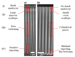
Whilst the nature of Bosch process etching with always result in scallops, the scallops have been greatly reduced. Changes in radius along the length of the pores have also been reduced to almost nothing. The result is a robust, reproducible etch which is well suited to the photonic crystal fabrication needs in the COPS group.
Abstract
Periodic arrays of deep nanopores etched in silicon by deep reactive ion etching are desirable structures for photonic crystals and other nanostructure for silicon nanophotonics. Previous studies focused on realizing as deep as possible nanopores with as high as possible aspect ratios. The resulting nanopores suffered from structural imperfections of the nanopores, such as mask undercut, uneven and large scallops, depth dependent pore radii and tapering. Therefore, our present focus is to realize nanopores that have as cylindrical as possible shapes, in order to obtain a better comparison of nanophotonic observations with theory and simulations. To this end in our 2-step Bosch process we have improved the mask undercut, the uneven scallops, pore widening and positive tapering by optimizing a plethora of parameters such as the etch step time, capacitively coupled plasma (ion energy) and pressure. To add further degrees of control, we implemented a 3-step DREM (deposit, remove, etch, multistep) process. Optimization of the etching process results in cylindrical nanopores with a diameter in the range between 280 and 500 nm and a depth around 7 μm, corresponding to high depth-to-diameter aspect ratios between 14 and 25, that are very well suited for the realization of silicon nanophotonic structures.
The paper is entitled “ Deep reactive ion etching of cylindrical nanopores in silicon for photonic crystals” and is published in Nanotechnology, by IOP Publishing. It is availble open source at the publishers at: https://doi.org/10.1088/1361-6528/acc034 A copy of the paper is also available on the COPS website at: https://nano-cops.com/publications/article/deep-reactive-ion-etching-of-cylindrical-nanopores-in-silicon-for-photonic-crystals. It is also available on the ChemRxiv preprint server: https://chemrxiv.org/engage/chemrxiv/article-details/63905efd44ccbc0422114226
This work was done by Melissa Goodwin, Cock Harteveld and Willem Vos of the Complex Photonic Systems (COPS) group of the MESA+ Institute for Nanotechnology at the University of Twente in the Netherlands and Meint de Boer of the MESA+ Nanolab of the University of Twente in the Netherlands. The work is part of the ongoing NWO-TTW Perspectief program “Free-form Scattering Optics” (FFSO), a collaboration in applied sciences and technology with TU Eindhoven and TU Delft, with active participation of users from leading industries ASML, Lumileds, Signify, TNO, Demcon, Schott.
Learn more about it here.